
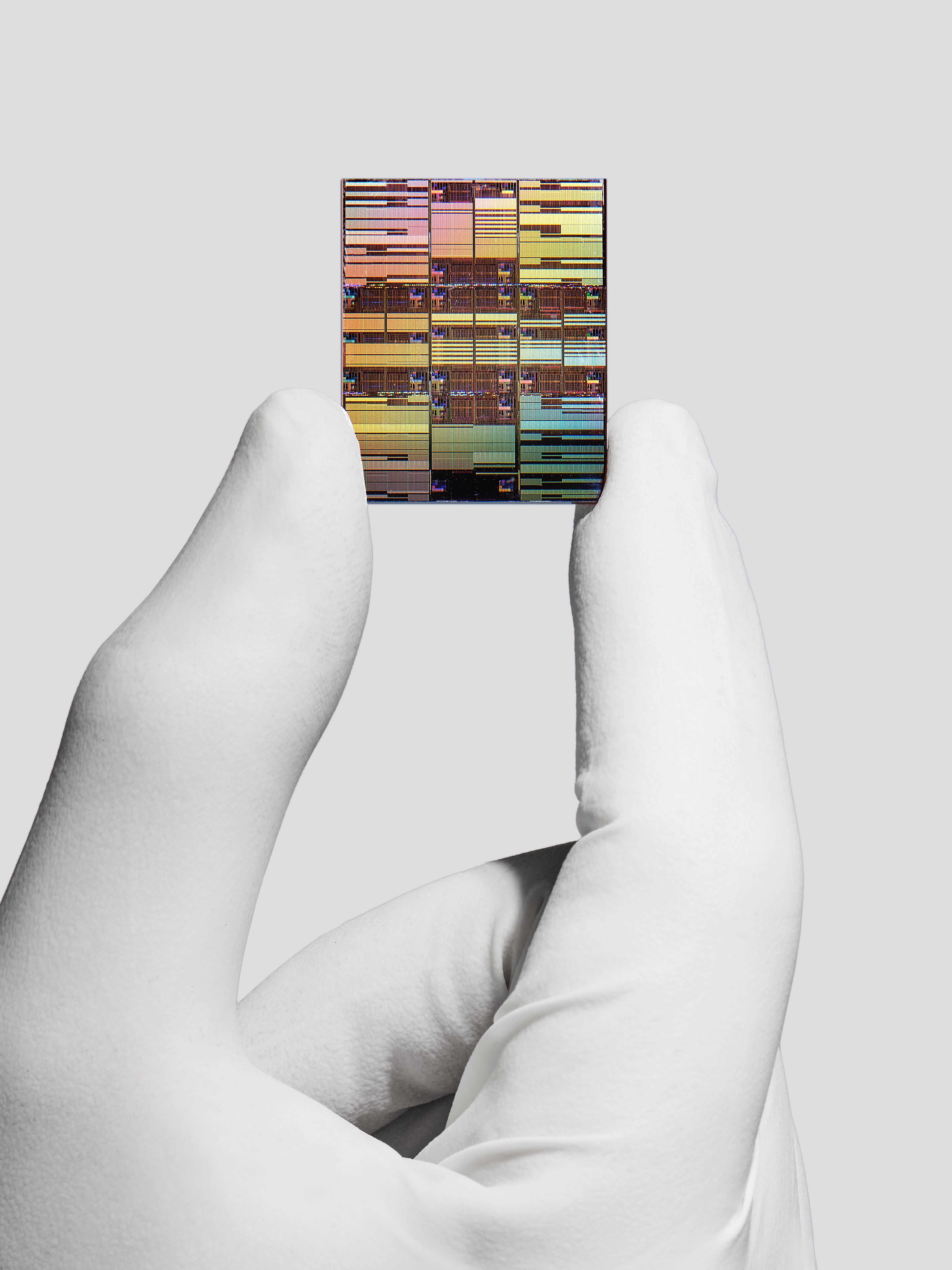
IBM presents first sub-1-nanometer chip, the size of a fingernail with 100 billion transistors
Translated from Spanish, summarized and contextualized by DistantNews.
At a glance
News
Sources not specified
New plan
- IBM has developed a new chip architecture capable of producing chips smaller than 1 nanometer.
- The new 'nanostack' technology allows for stacking transistors vertically, doubling density compared to previous 2-nanometer chips.
- This advancement promises significant improvements in performance and energy efficiency, with potential applications in various electronic devices.
IBM has unveiled a groundbreaking chip architecture that enables the creation of processors measuring less than 1 nanometer. This technological leap, utilizing a novel 'nanostack' design, represents a significant advancement in miniaturization, performance, and energy efficiency for semiconductor technology.
The new nanostack architecture builds upon the existing nanosheet technology. It involves stacking and staggering nanosheet transistors vertically, interconnected by a simple dielectric link. This three-dimensional approach is complemented by innovative methods for managing electrical current and new materials for the gate, which independently controls the flow of electricity to each transistor. Unlike previous designs, nanostack connects both the front and back of the transistors to the current independently.
IBM has successfully designed a chip measuring 0.7 nanometers (or 7 angstroms) using this architecture. This chip, roughly the size of a fingernail, reportedly contains nearly 100 billion transistors, effectively doubling the density achieved with IBM's 2-nanometer chip introduced in 2021. The company projects that this new design will boost energy efficiency by 70% and enhance performance by 50% compared to the earlier 2-nanometer chip.
IBM envisions this nanostack technology being applied across various chip types, including GPUs, CPUs, and processors. Potential applications range from powering more intelligent devices to enabling more efficient data centers. While the company still needs to refine the architecture, its roadmap suggests that mass production could begin within the next five years, paving the way for widespread adoption of this next-generation semiconductor technology.
DistantNews Editorial
Originally published by La Nación in Spanish. Translated, summarized, and contextualized by our editorial team with added local perspective. Read our editorial standards.
More Stories


From Our Blog

What Gets Lost (and Found) When News Is Translated

The Critical Role of Diaspora Media in Global News

What Travellers Should Know About Countries with Restricted Press

A Digital Nomad's Guide to Following Local News

How the Same Story Looks Different in Different Countries
